The F-11 (code name: the Fonz) was DEC's second microprocessor design, and the first to be architected in part by DEC personnel. Duane Dickhut was the project leader, Bill Johnson was lead design engineer for the Data chip, and Burt Hashizume wrote most of the microcode. The physical design of the Control and Data chip was done by Precision Micro Design, a consulting company set up by Western Digital veterans of the LSI-11. The MMU was designed by Dan Dobberpuhl's consulting company. (A tip of the hat to John R Wallace of PMD for providing more details on the design of the F11.)
The F-11 was substantially more ambitious than the LSI-11. It implemented the entire PDP-11/34 architecture, including FP11-compatible floating point and KT11-compatibile memory management. It targeted 3X the performance of the LSI-11, at almost the same clock rate. It provided physical address extension out to 22b, the first system to do so after the PDP-11/70. It implemented the PDP-11 Commercial Instruction Set as an option; the only other implementation was for the PDP-11/44.
Like the LSI-11, the F-11 was a chip set consisting of three designs, one of which could be replicated: the Control Chip (up to nine supported), the data chip, and the MMU chip. It was implemented in AMI's 6u NMOS process and operated at 3.6Mhz (280ns microcycle).
| Name | Number | Size | Transistors | Comments |
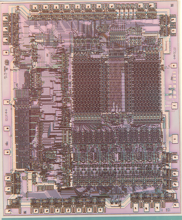
| Data | DC302 | 216x181 | 6,000 | The Data chip implements the instruction execution path of the F-11 chip
set. The Data chip operates under the control of microwords fetched from
the Control chip(s). Its key features are:
Power: 1.5W |
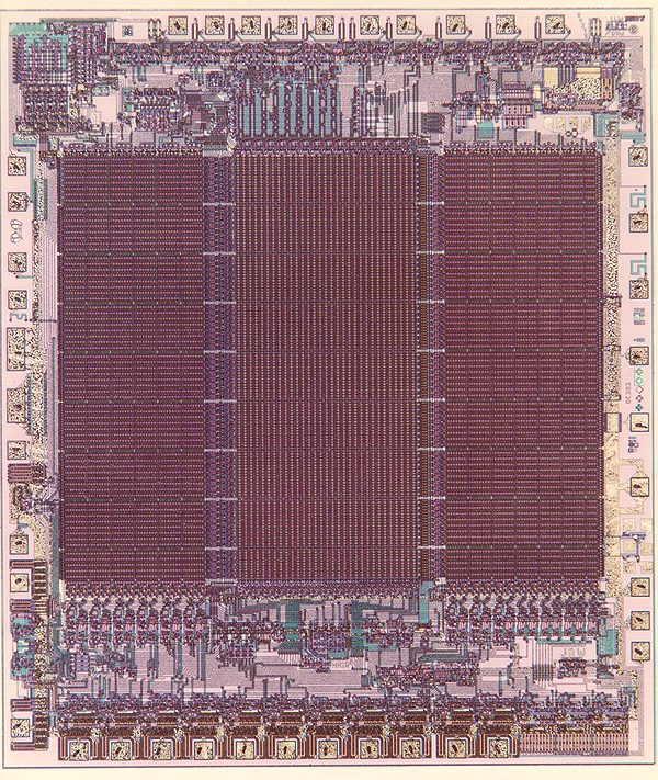
| Control | DC303 | 200x173 | 23,000 sites | The Control chip implements the microword access and sequencing functions
of the F-11 chip set. Its key features are:
Power: 1.0W |
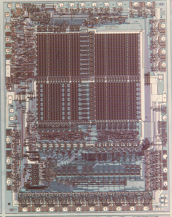
| MMU | DC304 | 250x196 | 10,000 | The MMU implements the memory management data path and controls for the
F-11 chip set. It also contains the PDP-11 floating point accumulators
and status registers. Its key features are:
Power: 1.5W. |
The F-11, like its predecessor, was very successful. In addition to expanding the penetration of PDP-11's in embedded and OEM markets, the F-11 was the basis of the LSI-11/23 (Qbus) and PDP-11/24 (Unibus) family of systems. DEC continued its tradition of second sourcing its designs by importing AMI's technology into its semiconductor fabrication facility.
I joined Small Systems Engineering's chip team in late 1978, when the Storage group I worked in transferred to Colorado Springs. For the first six months, I worked as an individual contributor, writing a strategic position paper on future chip directions and finishing half of the CIS microcode (the packed instructions). The position paper recommended a design project to build one more generation of PDP-11 microprocessors and an advanced development project focused on building a VLSI VAX. This recommendation was accepted, and I became the project leader for the last PDP-11 microprocessor, J-11.
Updated 13-May-2022 by Bob Supnik (simh AT trailing-edge DOT com - anti-spam encoded)